Tag Archives: PCB process

How to Solve AD20 Channel-Offset Error

preface

Solution to Channel-Offset Error when the same circuit module of ad20 PCB is multiplexed in room format

1. Problem phenomenon

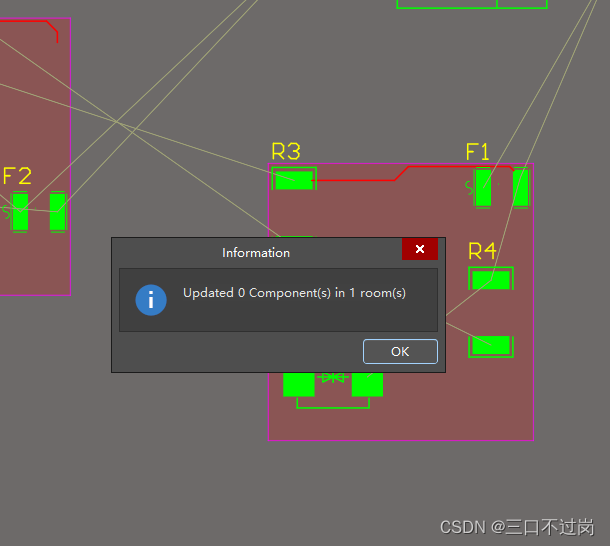
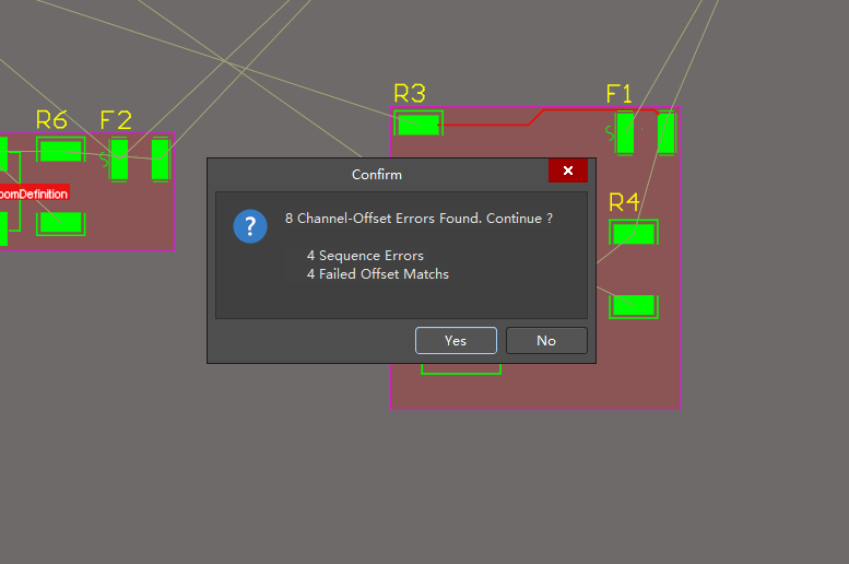
We often encounter the following problems when using room format to quickly layout circuits of the same module,

2. Solution

There are many processes of copying PCB layout of the same module circuit on the Internet, which will not be repeated here. The steps are similar, only the root cause of the problem
1: check whether the following three status settings are correct or not?
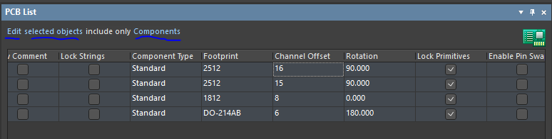
2: Channel Offset I recommend using the box, that is, select the first table and then pull down, paste the same; if you are in accordance with the EXCEL table as click Channel-Offset, and then right-click to copy, the results may lead to no copy success;.

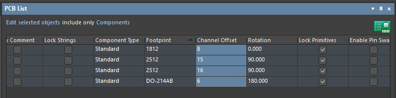
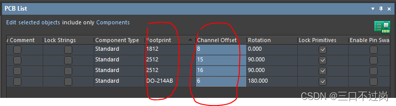
3: before pasting, pay attention to keep the device arrangement order of the original circuit and the target circuit consistent

my main problem is the second point. I thought the copy was successful, but I didn’t copy it, so I didn’t paste it. Finally, I kept reporting errors, which annoyed me!

Update ad schematic to PCB, failed to match

*Background: in the process of updating the schematic to PCB, there is often a mismatch between the components on the schematic and those on the PCB, so we should be very careful and check them one by one, otherwise there will be a lesson of blood and tears (the components in the PCB are lost).

1、 Update the schematic diagram to pcb
II. Perform device matching

There are automatic and manual. For the time being, demonstrate manual operation

for example: C35, find the first column and the second column, then select and click & gt

perform operations similar to C35 one by one

3、 Execute the change

in this figure, the remove operation is to delete the routing

in this figure, the remove operation is to delete the device

Do this carefully. You’d better take a picture, and then check whether any devices are lost one by one Is there any wiring missing!!!

Summary:
(1) this situation is generally caused by the person who changed the drawing before, just for a moment, directly changed the PCB without changing the schematic diagram or updating it
also, the PCB library path corresponding to the device is not specified.

(2) If a lot of network nodes are gone and the routing is gone as soon as the update is executed, it is the layout engineer’s method of drawing lines without nodes in pcbdoc!!!

Problem: error (24) file not found is prompted when importing the network table

A new PCB is created, and the following error is prompted when importing the network table:

  ERROR(24) File not found  

         Packager files not found

And

ERROR(102) Run stopped because errors were detected

This is because of the path problem. The path address in the red box below must be placed in the folder of the three files in the network table.