*Background: in the process of updating the schematic to PCB, there is often a mismatch between the components on the schematic and those on the PCB, so we should be very careful and check them one by one, otherwise there will be a lesson of blood and tears (the components in the PCB are lost).
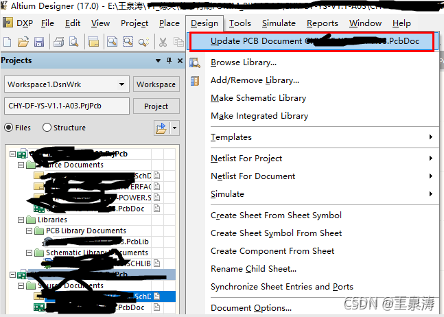
1、 Update the schematic diagram to pcb
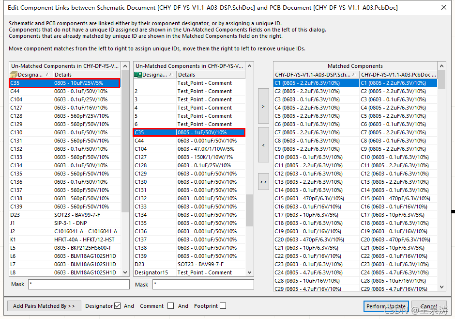
II. Perform device matching
There are automatic and manual. For the time being, demonstrate manual operation

for example: C35, find the first column and the second column, then select and click & gt

perform operations similar to C35 one by one
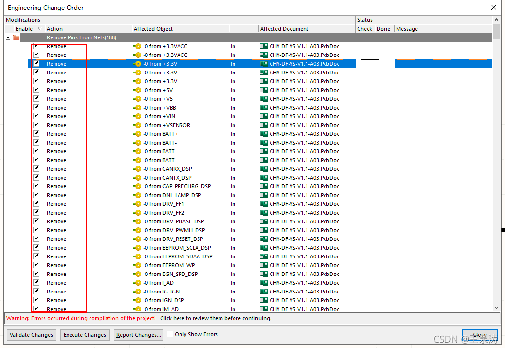
3、 Execute the change

in this figure, the remove operation is to delete the routing

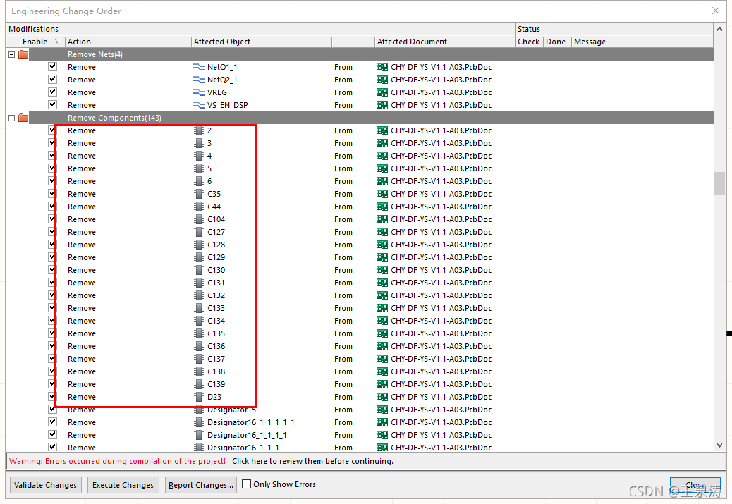
in this figure, the remove operation is to delete the device
Do this carefully. You’d better take a picture, and then check whether any devices are lost one by one Is there any wiring missing!!!
Summary:
(1) this situation is generally caused by the person who changed the drawing before, just for a moment, directly changed the PCB without changing the schematic diagram or updating it
also, the PCB library path corresponding to the device is not specified.
(2) If a lot of network nodes are gone and the routing is gone as soon as the update is executed, it is the layout engineer’s method of drawing lines without nodes in pcbdoc!!!